- This will not cause heat damage to surface because of backside only heat treatment.
- This is possible to control 1-10μm depth of anneal treatment by 2 waves laser.
- This is possible to achieve high throughput by combination of continuous vibration and turning table.
2 wavelength laser anneal
- Entering depth of laser to Si depends on wavelength.
- It is possible to raise temperature up to the necessary degree which let dopant activate in the area of some μm depth with keeping temperature of the un vibrated surface lower than 100 degree C even for the thin Si wafer which thick is lower than 100μm by vibrate 2 wave laser such as 1μm and 10μm length trespass.
- 拡大
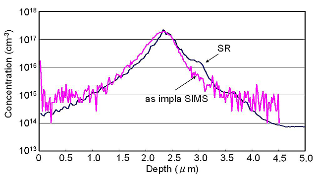
- Anneal data
1.Heat treatment backside only.
2 laser are installed such as green laser as well as LD and this has the following characteristics by vibrating those two laser simultaneously.
- It is possible to activate profile of various impurities at the depth of 10μm lower.
- It is possible to treat thin wafer such as lower 100μm.
- It is possible to maintain the surface temperature lower than 100 degree C at at the time of backside anneal.
2.High through put process
- It realizes active backside some μm anneal with high through put and keeping low temperature of surface by CW green laser, CW semiconductor laser and speed controlled stage.
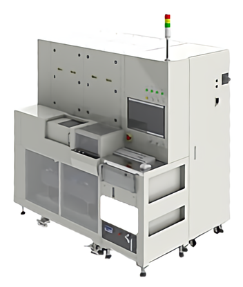
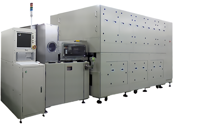
- The first ohmicization machine for backside electrode.
- It is applicable for development and prototype because of plenty of parameter.
- It support mass production by high stability, reproducibility, throughput and low running cost.
-
Ohmicization of various metal which is used for backside electrode of SiC.
| Ohmicization | Resistance :10~{-4}~10~{-6}Ωcm~{2} |
|---|---|
| High throughput | 5pieces/Hour ※6 inch wafer |
| Temperature control of non laser vibrated surface. | Lower than 120 degree C |
| Plenty of parameter. | Applicable to various type of electrode. |
| High precise area anneal | Applicable to atrundome size of wafer to 6 inches. |
| Running cost | Law utility cost. |
| Size of wafer | <6 inchs |
|---|---|
| Thickness of wafer | >100μm |
| Wafer allignment | Image recognition・Edge detection・Patern detection・Autofocus |
| Optical management | Laser power meter、Beam profiler |
| Wafer delivery mechanism | Lift pin |
| Anneal atmosphere | Class 1000 or N₂ |
| Safety control | Full cover・Interlock |
| Basic size (mm) | W2100×D1400×H2000(All inclusive) |
- For thin wafer (100μm<50μm)
- Automatic delivery system
- Noncontact wafer hold system (Robot hand)
- The higher pure degree
- Corresponding to CIM
Inquiries about laser business.
ENGINEERING DEPT.1
Call: +81-42-542-7100